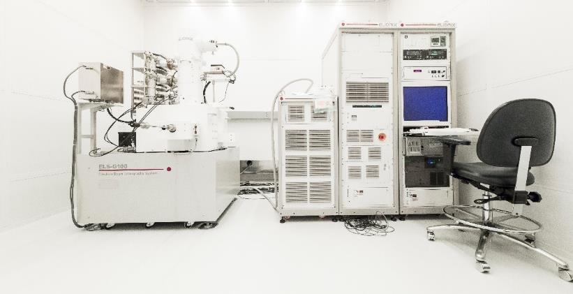
About The Origin of Electronic Beam Lithography
Electron-beam technology has provided the basis for a variety of novel and specialized applications from the mid-20th century. Electron Beam Lithography is one of them. Electron-beam lithography (abbreviated as e-beam lithography, EBL) is defined as the process of scanning a focused beam of electrons to display custom shapes on a surface having a covering of an electron-sensitive film called a resist.
EBL is known for its special technique for the creation of extremely small fine patterns (can’t be seen from the naked eye) applied usually in modern electronics applications for integrated circuits. This Electron Lithography System is more suited to create exclusively the high-resolute patterns, or some unique patterns for which the other process such as the creation of photomask is very much time consuming.
Principle of Electronic Beam Lithography
The Electron Beam Lithography System works on a principle that is somewhat related to photolithography. When the focused beam of electrons scanned over a surface called resist. It changes its solubility properties in accordance with the energy deposited with the electronic beam.
About Resolution
In electron beam lithography resolution, the resolution is primarily set by the electronic beam. This is further depending on the range of electron interaction phenomena forming the custom designs. The Electron beams can produce structures of 1 nm in size and useful devices with minimal features of about 20 nm. The electronic beam can be as small as 0.5 nm. All useful devices have an ultimate resolution of about 10 nm. 10 nm is the direct resolution of materials such as AlF 3 and Al 2 O 3; 1-nm structures. In the processes where the intermediate patterned layers are used, made by the direct modification of the electrical properties of conductors, semiconductors, or superconductors by means of high-energy electron bombardment. In these cases, no type of fabrication process is used, this would further reach dimensions comparable to the beam diameter.
Applications of Electronic Beam Lithography System
- Electron Beam Lithography systems are capable of high resolution custom patterns on a surface called resist.
- This technique seems flexible towards a variety of materials and an infinite number of patterns.
- This is somewhat a slow technique being one or more orders of magnitude slower than optical lithography.
- This technique is on a costlier side and is considered expensive. Since providing highly resolute custom patterns, all which requires tools that can cost many millions of dollars and requires frequent services to stay properly maintained.
- Electron beam lithography can manufacture tiny nanostructures with high reliability and accuracy, without the need for a photomask, and at a resolution of less than 10 nm.
- More suited to create unique and highly resolute patterns for which photomask is too time consuming or wasteful.
- Electron source use in this Electron Beam Lithography System is Hot W/ZrO2 used for the electron emission, or for the magnetic lenses to focus the beam. Resist layer is configured and creates the complex trough shapes such as T-shape or stepped.
- To adjust the solubility of resist over greater or lesser volume, multiple layers of different sensitivity are induced via electronic beams. Scattering, diffusion or secondary electronic production
- A finely focused (sub-micrometer diameter) electron beam is used for writing patterns in thin films of electron sensitive material.
- This system can generate very complex patterns with great accuracy, highly resolute integrated circuits techniques are used for generating the masks that are projected optically on a silicon sheet coated with the photosensitive resists.
- In the process of electron beam lithography, materials are exposed to the intense beam of electrons but these electrons in the process are grounded safely in order to avoid any charging effects. Grounding is done by adding a thin layer, aluminum or gold between the resist and the substrate or on the top of the resist.
- Now operating an EBL machine is easy as it is not required to understand the underlying math and physics behind the technique. Due to the advancement of computer systems, it allows easy and accurate design of optical components and columns.
- STS-Elionix, partnership that is delivering the state of the art nanotechnology products by linking the electron beam lithography system with the computer system and is meeting the customer demands for finer lines and writing speeds.
- STS-Elionix invented the world’s first 150Kv EBL system for research as well as the world’s first 400MHz beam deflection system with the help of EBL tools.
- Electron-beam lithography systems when used in commercial applications use e-beam writing systems that are very expensive (> US$1M).
- For research applications, it gets converted into an electron microscope to an electron beam lithography system using relatively low cost (< US$100K). Such converted systems have produced linewidths of ~20 nm during 1990, while current dedicated systems have produced linewidths on the order of 10 nm or smaller.
- Both electrostatic and magnetic lenses are used in the Electron Beam Lithography system.
- Given the high resolution of electron-beam lithography, there are generations of defects during electron-beam lithography that are often not considered by users. Defects that occur are classified into two categories: data-related defects, and physical defects.
Many of the companies like SEMTECH, Multibeam Corporation, Mapper, IMS Nanofabrication are practicing to regenerate and are working to update the electronic beam technology by using various research and productive tools.

